 Follow Us
 The AD9361 and AD9371 RadioVerse™ wideband transceiver families both offer an unparalleled level of integration, as well as a plethora of features and many user-selectable options. The two families have significantly different levels of performance in several key areas and power consumption is also quite different between the two product families. Image rejection is one of the areas of performance that differs between the two families. This article explores where images come from, what they are, and how they impact overall system performance. Armed with that information, customers can make informed decisions and select the right transceiver for the application.
Image Rejection Basics
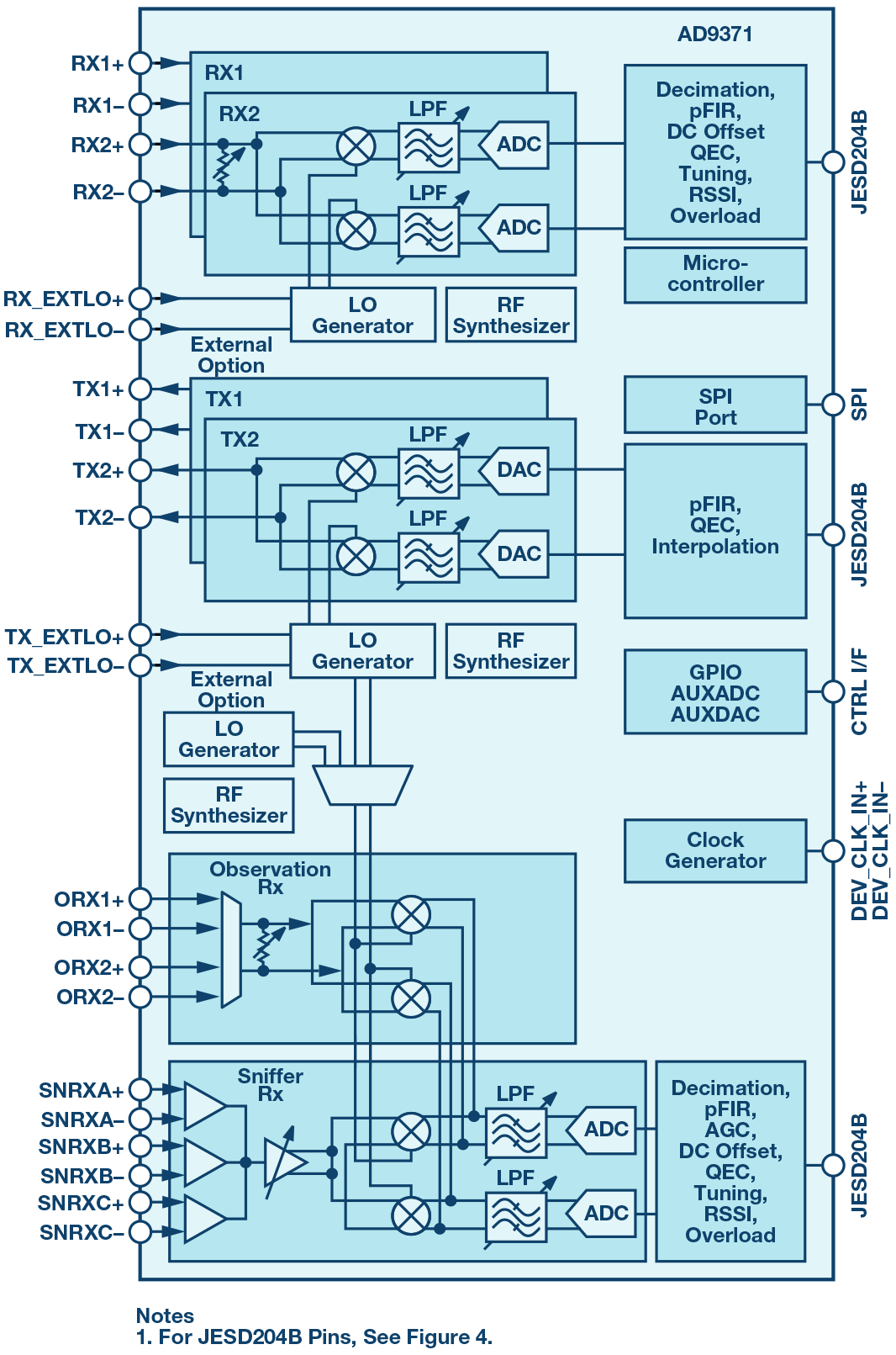
Both the AD9361 and AD9371 families use zero intermediate frequency (aka, zero-IF or ZIF) architectures, which results in a very high level of integration and significantly reduces the number of frequency-dependent components in the system. As shown in the block diagram of the AD9371 in Figure 1, both the main receive and transmit signal paths use one complex mixer stage to translate between the radio frequency (RF), which is centered around the local oscillator (LO) frequency, and baseband, which is centered around dc. For an excellent starting point to understanding the complex mixers used in ZIF transceivers, refer to the article on complex RF mixers referenced at the end of this article.1
While providing many advantages due to such high integration, ZIF radios bring challenges as well. A complex mixer has in-phase (I) and quadrature-phase (Q) signals. Any mismatch of phase or amplitude of those signals degrades the summing and cancellation that occurs when the upconverted I and Q signals are combined. This is described in the article referenced above. Imperfect cancellation results in an inverted copy of the desired signal appearing on the opposite side of the local oscillator (LO) frequency from the desired signal when transmitting. This copy is referred to as an image and has a reduced amplitude compared to the desired signal. Similarly, an inverted copy of the desired signal appears on the opposite side of dc from the desired signal when receiving. In some other architectures (for example, super heterodyne), this image can be filtered at an intermediate stage. The primary advantage of the ZIF architecture is the removal of those filters and the intermediate mixer stage, but this necessitates very good I and Q balance to reduce the image amplitude to an acceptable level.
The simplified diagram of a receive signal path in Figure 2 shows where these mismatches occur with the mismatches designated by ΔA, ΔfC, and Δφ. Only one path shows the added factors since it is the imbalance between the signal paths that creates the image, not the absolute gains and phases of the signal paths. Therefore, it is mathematically correct to show all of the imbalance factors in just one of the paths. The complex mixer shown in Figure 2 is also known as a quadrature mixer since the two LO signals provided to the mixers are orthogonal to each other.

Figure 3 shows an example using a single-tone or continuous wave (CW) desired signal and the resulting unwanted CW image. The desired signal is downconverted to frequency ωC. If the quadrature balance is not perfect, the image will appear at frequency –ωC. The image rejection radio (IRR) is the difference in dB between the desired signal and the unwanted image signal. Reducing the quadrature balance is known as quadrature error correction (QEC).

The image amplitude is related to the gain and phase mismatch by the following equation:

Where:
Δ = the normalized amplitude imbalance. To cancel two signals, they ideally need to be 180° out of phase and have the same amplitude. The “d” in cos(d) represents the phase deviation of the two signals from each other. 0 is ideal. 1° means that one signal deviates by 179° instead of 180. If one signal’s amplitude is 1 and the others is 0.99, then the delta is 0.99.
θ = the phase error in degrees (a value of zero is ideal)
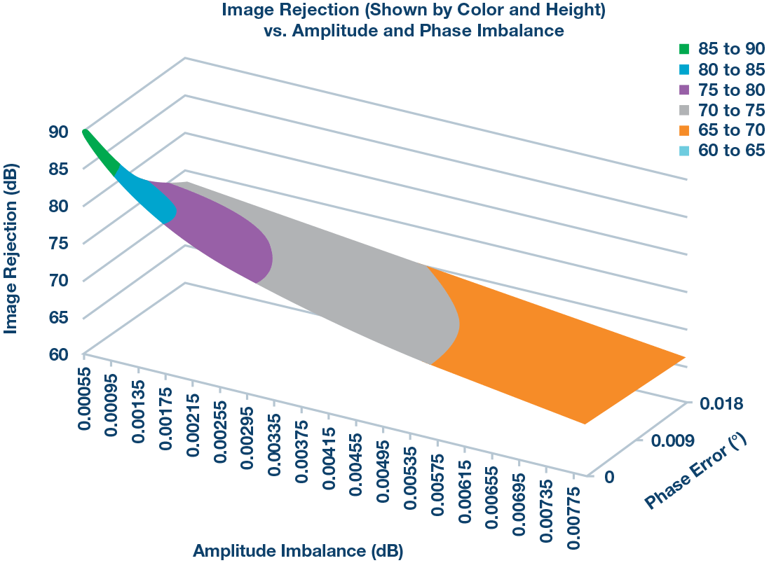
Equation 1 results in a two-dimensional matrix since image rejection will be degraded by both input variables independently. A portion of this matrix is shown in Figure 4, where the axis across the page is amplitude imbalance, the axis into the page is phase imbalance, and the vertical axis is the image rejection in dB. For example, if a 0.00195 amplitude error exists and the system needs to achieve an image rejection of 76 dB, the phase error must be better than 0.01286°. Even within a single integrated circuit device, it is very difficult to reach an image rejection better than 50 dB by controlling all of the factors that affect the I and Q matching. Achieving the 76 dB image rejection typically achieved with the AD9371 requires digital algorithms to manipulate analog path variables and to apply correction in the digital domain.
The Effects of Images on Desired Signals
Figure 5 shows a simplified drawing of a single carrier case with the waveform centered at dc after downconversion. An example of this waveform would be a single instance of a 20 MHz LTE downlink OFDM signal. As seen in Figure 5, a portion of the desired signal on the negative side will have an image on the positive side and vice versa. In the single carrier case centered on dc, the image lands within (or on top of) the desired signal and corrupts the desired signal.
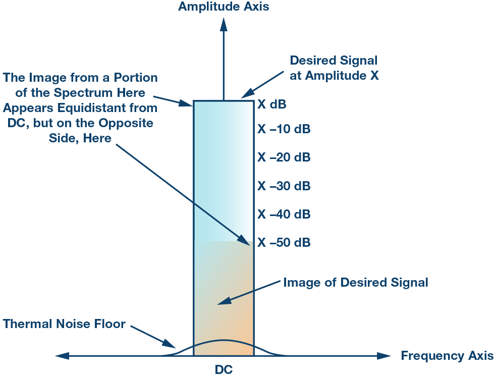
When receiving and then demodulating a signal, there are several impairments that will be present. Thermal noise, which increases the noise floor of the receive signal path, is one example. Images add noise as well if they land within the desired signal. If the total of all noise sources is too high, then it will not be possible to demodulate the signal. The thermal noise floor shown in single carrier and multicarrier figures is an example and in these discussions is ignored as a contributor.
When using the AD9361’s internal LO that is suitably supplied with a reference clock source with the recommended performance, the AD9361 will achieve approximately –40 dB EVM when not noise-floor limited. The EVM is limited to –40 dB by the phase noise of the RF PLL. The AD9361 image rejection performance of approximately 50 dBc means that in the single carrier case shown in Figure 5, the image alone will only degrade EVM by approximately 0.5 dB. Such low EVM degradation means that the transceiver will typically not be a limiting factor with modulation schemes such as 64-QAM and even higher. In this single-carrier case, the image is always smaller than the desired signal by approximately 50 dB and as shown in Figure 5.
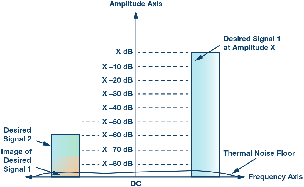
Figure 6 shows a multicarrier example. Here, the desired signals are offset from dc after downconversion.
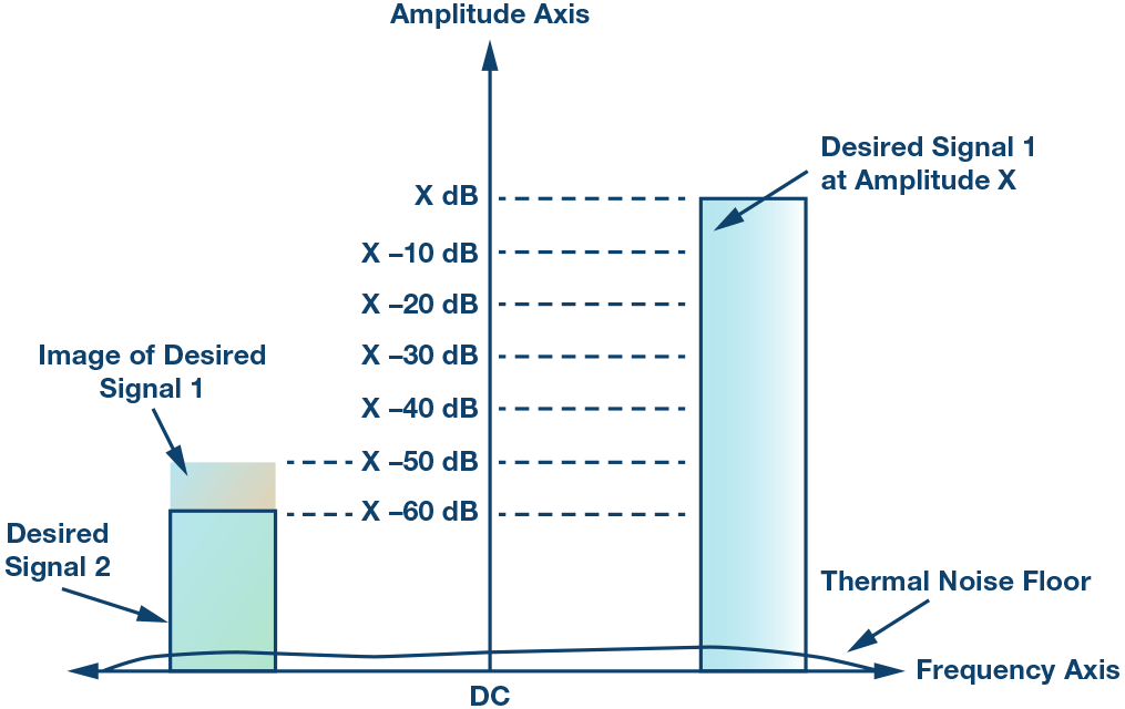
The image of each desired signal reflects through dc and shows up on the opposite side of the spectrum. In this example, two desired signals have been downconverted to the same offset from dc, desired Signal 1 on the positive side, and desired Signal 2 on the negative side. Note that the amplitude of desired Signal 2 is 60 dB below the amplitude of desired Signal 1. Two carriers with differing amplitudes is a common occurrence in multicarrier cases that arises when the signals from two mobile stations encounter different amounts of path loss when traveling to the same base station. This can occur when the two stations are different distances from the base station or one station transmits through or around different objects than the other station.
The amplitude of desired Signal 2 is 10 dB lower than the image from desired Signal 1. This represents a signal-to-noise ratio for desired Signal 2 of –10 dB. Demodulation, even using the simplest modulation techniques, would be extremely difficult if not impossible. Clearly, better image rejection performance is needed to handle these scenarios.
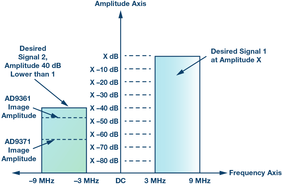
Figure 7 shows the same scenario but with receive image rejection performance typical of the AD9371.
The image from desired Signal 1 now lies 15 dB below the amplitude of desired Signal 2. This provides 15 dB of signal noise ratio, which is enough to demodulate desired Signal 2 using a variety of modulation schemes.
Techniques Reducing Quadrature Imbalance in the AD9361 and the AD9371
Both the AD9361 and the AD9371 have optimized analog signal and LO paths that inherently reduce quadrature imbalance. As mentioned above, however, there is a limit to what good silicon can achieve. Digital correction can improve image rejection by several orders of magnitude.
The AD9361 receiver quadrature calibration uses an algorithm that analyzes the entire received spectrum of data to create an average correction across the entire bandwidth. For single-carrier use cases and relatively narrow bandwidth such as 20 MHz, this correction yields good image rejection across the bandwidth of interest. This is referred to as a frequency-independent algorithm. The algorithm operates on received data and updates in real time.
The AD9371 runs receive image rejection calibrations both during initialization by injecting test tones and during operation using actual received data. These more advanced calibrations adjust for frequency-dependent imbalance as well as frequency-independent imbalance. The algorithm updates in real time. The more advanced algorithm and circuitry that implements the corrections yields performance approximately 25 dB better than the AD9361 across the occupied signal bandwidth.
This article demonstrates the origination and effects of quadrature imbalance using the receive signal path, but a ZIF transceiver must overcome the same issues in the transmit signal path as well. The output of the transmitter includes both the desired signals as well as their images when the signal path or the LO paths are imbalanced.
For the transmit signal path, the AD9361 uses an initialization calibration to reduce quadrature imbalance below that provided by the optimized hardware design. The calibration uses a CW tone placed at a single frequency and at a single attenuation setting. The algorithm typically results in an image approximately 50 dB below the power of the desired signal. Another way to write this would be –50 dBc (decibels below carrier). Operation over temperature, across a wide bandwidth, or at different attenuation settings can affect the image level.
The AD9371 uses an initial transmit path calibration using many internally generated tones spread across the desired signal bandwidth and it determines the correction factors across multiple transmit attenuation settings. During operation, a transmit signal path tracking calibration uses real transmitted data and periodically updates the correction factors during operation. The AD9371 achieves approximately 15 dB better image rejection compared to the AD9361 and it provides this benefit over temperature, attenuation, and across the occupied signal bandwidth.
A Simplified Specific Example
Using all that has been covered in this article so far, let’s perform a thought experiment and assume that we are building a system in which there is a central base station and multiple client devices. To simplify the example, the system will be operating away from objects such as buildings that cause multipath. The base station is expected to communicate with the client devices that can be spread throughout an area with a radius of 100 meters, as shown in Figure 8.
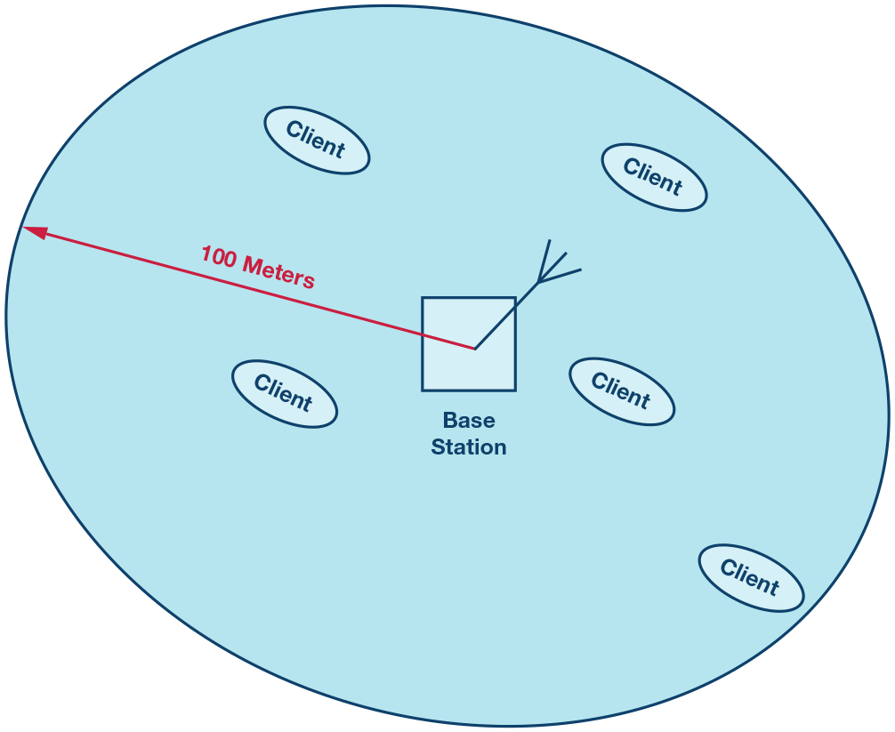
The system will use multiple, simultaneously transmitted, 6 MHz wide carriers across a total bandwidth of 18 MHz. Let us say that in this system, one client unit could be very close to the base station—say, 0.3 meters—while the farthest could of course be 100 meters away. The free space path loss difference between the two would be approximately 50 dB. Let us also assume that the base station baseband processor can measure the received power and then tell the client to increase or decrease its transmit power by up to 10 dB. A nearby client would decrease by 10 dB while a client at the far end of the range would transmit at full power. This reduces the received power at the base station by 10 dB, resulting in an overall potential difference of 40 dB, as shown in Figure 9. The two displayed carriers represent the worst-case situation described above. For clarity, the optional carrier that could reside between the two desired signals has been omitted.

In this system, we will assume that the same transceiver will be used for both base station and client. If the AD9361 is used, the transmitted image can be approximately 50 dB below the amplitude of the desired signal. The receiver will also add a similar amount of image power. The two quadrature imbalances combine to create an image approximately 47 dB below the desired signal.
If the AD9371 is used for both ends of the link, then the transmitted image would typically be 65 dB down and the receiver would contribute an image 75 dB down below the desired signal. Adding those two up results in a total image of approximately 64.5 dB below the desired signal. Figure 10 shows both results.
In this simplified example, we are considering only the effects of the image and ignoring influences on SNR such as thermal noise, phase noise, and nonlinearities. Here, the AD9361 case results in an SNR of approximately 7 dB while the AD9371 case results in approximately 24.5 dB of SNR in this example. If complex modulation schemes such as 64-QAM are used in this system, then the total system SNR requirement would probably make the AD9371 the best choice. If simpler modulation schemes are used, such as QPSK, the AD9361 may be more than adequate. Techniques used in the baseband processor would determine the actual system SNR needed to demodulate the signal. And, of course, to move from this thought experiment to a real system, the effects previously ignored such as thermal noise would have to be considered.
Conclusion
The previous plots and description of the quadrature correction algorithms in the two transceivers focused on the receive signal path. The effects of undesired images also apply to the transmit path for the same reasons. A transmission image that lands on top of a smaller carrier is equally troublesome for the station receiving the signals.
The section describing the techniques used by the transceivers to reduce image level shows the quantitative differences achieved by the two different families of devices. Then the specific example above takes us through a system design and narrows the design decision down to a few concise questions about the SNR required to demodulate the received signal. While the AD9371 family will always have better image performance than the AD9361 family, the higher power consumption of the AD9371 family and the use of a high speed serial interface require system engineers to look at all aspects of the design and find the best solution for their application.
