 Follow Us
 Abstract
This article aims to help hardware designers with the design of wide bandwidth programmable gain instrumentation amplifiers (PGIAs) from the selection of off-the-shelf discrete components to performance evaluation and how to save time and reduce design iterations. The PGIA architecture presented is optimized for driving the high precision successive approximation register (SAR) architecture-based signal chain at full speed. The article also demonstrates the PGIA’s precision performance in driving wide bandwidth signal chains for various gain options.
Introduction
A precision data acquisition subsystem typically consists of high performance, discrete linear signal chain blocks to measure and protect, condition and acquire, or synthesize and drive. Hardware designers developing these data acquisition signal chains typically require high input impedance to allow direct interface with a variety of sensors. In this case, a programmable gain is often needed to adapt the circuit to different input signal amplitudes—unipolar or bipolar and single-ended or differential with varying common-mode voltages. The majority of PGIAs traditionally consists of a single-ended output that cannot directly drive a fully differential, high precision SAR architecture-based signal chain at full speed and may require at least one signal conditioning or driver stage. Industry dynamics have been rapidly evolving with increased focus on system software and applications to differentiate system solutions. There is less time to build and prototype analog circuits to verify their functionality due to tight R&D budgets and time to market constraints. Hardware development resources are put under increased pressure to reduce design iterations. This article focuses on the key aspects of designing a discrete wide bandwidth, fully differential PGIA and demonstrates its precision performance when driving a high speed signal chain μModule® data acquisition solution.
PGIA Design Description
Figure 1 shows the discrete wide bandwidth, fully differential PGIA simplified circuit block diagram. The key specifications and design requirements for this PGIA circuit are listed in Table 1.
| PGIA Specification | Design Requirement | Comments |
| Output Common Mode | 2.048 V | Fixed |
| Differential Output to ADC | 8.192 V p-p | Fixed |
| Gains: Single-Ended or Differential | 2, 10, 64, 128 | Programmable |
| Supplies +VS/–VS | +15 V/–15 V, –6 V/–2 V | A single supply of 5 V can be used for FDA (trade-off: 3 dB to 4 dB SNR drop) |
| Bandwidth | >50 MHz | Required to drive SAR device at 15 MSPS |
| Noise | <2 nV/√Hz | Required to achieve SNR above 85 dB |
| Offset Voltage Drift | ≤2 µV/°C | Overall lower drift reduces calibration burden in system |
| CMRR | >90 dB for all gains | |
| Signal Chain Specification | ||
| µModule Fully Differential | 16-bit/18-bit | |
| µModule Sample Rate | 15 MSPS | Lower sample rate can be used if desired |
| SNR at 100 kHz | >85 dB at G = 2, >73 dB at G = 128 | Design target |
| THD at 100 kHz | <–105 dB at G = 2, <–70 dB at G = 128 | Design target |
This discrete PGIA is built using the following components:
- ADA4898-1 low noise, high speed amplifiers
- LT5400 quad matched resistor network, used as gain and feedback resistors to set PGIA gain
- ADG1209 low capacitance, iCMOS™ multiplexer to control PGIA gain
- ADA4945-1 wide bandwidth, fully differential amplifier (FDA)
The discrete components for this wide bandwidth PGIA circuit were chosen to meet the PGIA specifications highlighted in Table 1 and achieve an optimized AC and DC performance when driving fully differential high speed signal chain μModule data acquisition solutions such as the ADAQ23875 and ADAQ23878, and ADCs such as the LTC2387-16/LTC2387-18.


Design Tips and Components Selection
The ability of this wide bandwidth discrete PGIA solution to drive high speed SAR architecture-based signal chain μModule solutions and achieve optimized performance is dependent on the key specifications (such as bandwidth, slew rate, noise, and distortion) of the amplifiers as well as the FDA. The ADA4898-1 and the ADA4945-1 were chosen because their gain bandwidth (GBW) products support the overall bandwidth requirements of this signal chain. The ADA4945-1 (FDA) is only required when driving ADCs such as the LTC2387-16/LTC2387-18. The criteria for setting the PGIA gain are dependent on the selection of amplifiers, feedback resistors, and multiplexers, as discussed in the next section.
Setting the PGIA Gain
Selecting Gain and Feedback Resistors
The gain and feedback resistors of the amplifiers should be precisely matched. The LT5400 quad resistor network offers 0.2 ppm/°C matching drift and 0.01% resistor matching over a wide temperature range as well as better common-mode rejection ratio (CMRR) than independently matched resistors. The gain resistors around the FDA also need to be matched precisely to achieve optimum CMRR performance. The LT5400 resistor network is used to set the gain of amplifiers. The gain computation is shown in equations 1 to 3.


By setting R1 = R4 and R2 = R3 when using the LT5400, the gain would be:

The gain of amplifiers and the FDA (fixed gain of 2) make up the total gain of the PGIA as shown in Table 2.
The LT5400 series has a variety of resistor options available as shown in Table 2. The ADG1209 multiplexer can be bypassed by using the amplifiers in a unity-gain configuration, so a total PGIA would be set to 2 in this case.
| Device | R2 = R3 (kΩ) | R1 = R4 (kΩ) | RGAIN (Ω) | ADA4898-1 Gain (V/V) | Total PGIA Gain (V/V) |
| LT5400-4 | 1 | 1 | N/A | 2 | 4 |
| LT5400-6 | 1 | 5 | N/A | 6 | 12 |
| LT5400-7 | 1.25 | 5 | N/A | 5 | 10 |
| LT5400-8 | 1 | 9 | N/A | 10 | 20 |
| LT5400-4 | 1 | 1 | 130 | 31.77 | 63.54 |
| LT5400-4 | 1 | 1 | 63.4 | 64.09 | 128.18 |
To set the gain higher than 20, an external precision matched gain resistor (RGAIN) is added between the inverting inputs of the ADA4898-1 amplifiers, and the LT5400-4 are used as feedback resistors to achieve a target gain of 64 and 128 as shown in Figure 2.
To compute the RGAIN value, refer to equations 4 to 8.


And the value of RGAIN for desired gain would be:

Selecting a Multiplexer
A multiplexer is used to control various gains of this PGIA circuit by selecting the LT5400 quad resistor network. When selecting a multiplexer for this wide bandwidth discrete PGIA design, the multiplexer’s important parameters such as on resistance (RON), on capacitance (CON), and off capacitance (COFF) should be considered. For this wide bandwidth PGIA design, it is recommended to use the ADG1209 multiplexer. The compensation capacitor (Cc) is added in the feedback path of amplifiers to minimize gain peaking and reduce the effect of the multiplexer on/off capacitance. The Cc along with the RON, feedback, and gain resistors will create a pole, which will compensate the effect of capacitive parasitic zero in the feedback loop gain. The Cc value should be optimized to achieve the desired closed-loop response. When a higher feedback resistor value is used around the ADA4898-1, more peaking appears in the closed-loop gain due to its high input capacitance. To avoid this issue, a higher feedback resistor value and feedback capacitor should be used in parallel around the ADA4898-1. The optimized Cc value of 2.7 pF is chosen here as recommended in the ADA4898-1 data sheet as shown in Figure 2. A smaller Cc will have minimal gain peaking, whereas too large of a Cc will affect the gain flatness of the closed-loop gain.


PGIA Power Supplies
Figure 3 shows the board used to evaluate the performance of this discrete wide bandwidth PGIA design.

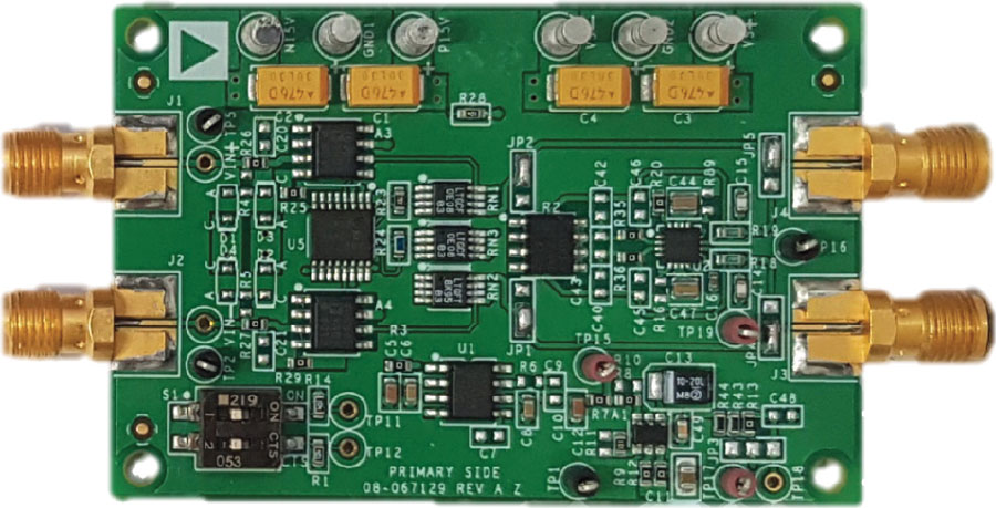
The ±15 V supplies are required to power up the PGIA front end that consists of two high speed ADA4898-1 amplifiers and an ADG1209 multiplexer, while the ADA4945-1 FDA requires 6 V and 2 V supply rails to achieve optimum signal chain performance. Although this board requires benchtop power supplies, the recommended LTpowerPlanner® power tree and current drawn for each of the rails for this PGIA circuit are shown in Figure 4.


PGIA Performance
Bandwidth
Figure 5 shows the closed-loop gain vs. frequency plot for different gain settings. As the PGIA gain is increased from 2 to 128, its bandwidth will decrease while its noise referred to output (RTO) will increase; hence, the signal-to-noise ratio (SNR) will decrease.


CMRR
Figure 6 shows the CMRR vs. frequency plot for different PGIA gain settings.


Distortion
The Audio Precision® (APX555) signal analyzer is used to test the distortion performance of the PGIA board (Figure 4), and its output was set at 8.192 V p-p by applying various input voltage for various gain settings. Figure 7 shows the total harmonic distortion (THD) vs. the frequency performance of the discrete wide bandwidth PGIA.


Key Specifications Summary
A summary of key PGIA specifications such as bandwidth, slew rate, drift, and distortion measured on the bench using the discrete PGIA board (Figure 4) is shown in Table 3.
| PGIA Gain (V/V) | –3 dB Bandwidth (MHz) | Slew Rate (V/µs) | Drift (µV/°C) | THD (dB), FIN = 1 kHz |
| 2 | 47.7 | 77 | 0.06 | –126.5 |
| 10 | 12.99 | 72 | 1.18 | –116.11 |
| 63.54 | 2.15 | 10 | 0.042 | –110.04 |
| 128.18 | 0.98 | N/A | 0.026 | –103.32 |
A PGIA That Drives Signal Chain μModule Solutions
Figure 8 shows that the selected multiplexer input is followed by the two ADA4898-1 low noise, high speed amplifiers combined with the LT5400 quad precision matched resistor network that drives the ADAQ23875 signal chain µModule at 15 MSPS. The ADAQ23875 has an internal fully differential amplifier; thus, the FDA block of the wide bandwidth discrete PGIA board (Figure 4) should be bypassed. The Audio Precision (APx555) signal source is used for the evaluation of SNR and THD and in this case, the input amplitude was set around –0.5 dBFS.


Complete Signal Chain Performance
Noise
The dynamic range and referred to input (RTI) noise for a specific input range or gain setting of a complete signal chain (Figure 8) are shown in Table 4.
| PGIA Gain (V/V) | Input Range (V p-p) | Dynamic Range (dB) | RTI Noise (µV rms) |
| 2 | 4.096 | 87.68 | 59.85 |
| 10 | 0.819 | 79.39 | 31.05 |
| 63.54 | 0.129 | 78.85 | 5.20 |
| 128.18 | 0.064 | 76.83 | 3.25 |
The SNR performance vs. frequency of the discrete PGIA driving the ADAQ23875 is shown in Figure 9 when using the ADA4898-1 amplifiers. The overall dynamic range or SNR degradation due to the increase in PGIA gain is attributed to the inherent noise of individual resistors, amplifiers, and μModule solutions.
The precision performance of the ADAQ23878, combined with a high sampling rate, reduces noise and enables oversampling to achieve exceptionally low rms noise and detection of small amplitude signals over a wide bandwidth. In other words, a 15 MSPS sample rate greatly relaxes antialiasing filter requirements and maximizes bandwidth when digitizing fast transients and small signal levels. Oversampling refers to sampling much faster than twice the signal bandwidth required to meet the Nyquist criterion. For instance, oversampling the ADAQ23875 by a factor of four provides one additional bit of resolution or a 6 dB increase in dynamic range—in other words, the DR improvement due to this oversampling is defined as: ΔDR = 10 × log10 (OSR) in dB. The ADAQ23875 typical dynamic range is 91 dB at 15 MSPS for a 4.096 V reference with its inputs shorted to ground. For example, when the ADAQ23875 is oversampled by a factor of 256×, this corresponds to a signal bandwidth of 29.297 kHz and a dynamic range close to 111 dB for the different gain options, which can precisely detect small amplitude μV signals. Additional oversampling can be applied to trade off between noise and bandwidth to suit the measurement being performed.


Distortion
Figure 10 and Figure 11 show the THD performance of the signal chain (up to 100 kHz and from 100 kHz up to 1 MHz) when the ADAQ23875 is driven by the discrete PGIA. The THD gradually degrades as the PGIA gain and input signal frequency are increased since the bandwidth and slew rate of the ADA4898-1 start to deteriorate. Figure 11 also shows a THD performance comparison for two signal chains when the PGIA drives the ADAQ23875 vs. when the combination of the LTC6373 and ADA945-1 drives the LTC2387-16 at 15 MSPS.


Integral Nonlinearity (INL) and Differential Nonlinearity (DNL)
When the PGIA drives the ADAQ23875, it is also important that the overall DC accuracy of the signal chain is maintained. Figure 12 and Figure 13 show the typical INL and DNL performance with a PGIA gain of 2. For all other gain settings, INL and DNL stay within typically ±0.5 LSB.


Conclusion
This article features the design aspects of a discrete wide bandwidth PGIA built using the ADA4898-1 amplifiers, the ADG1209 multiplexer, and the LT5400 precision matched resistors. It showcases the high accuracy measurements of tens of millivolts to sub-10 volts single-ended/differential signals feeding into the 16-bit, 15 MSPS ADAQ23875 signal chain μModule solution. A complete signal chain offers an overall better precision performance than what can be achieved using the monolithic PGIAs available in the market. This wide bandwidth signal chain is tailored for a specific set of customers building test instruments used in automated test equipment, power supply monitoring, and analyzers.
References
Pachchigar, Maithil. “Increase Dynamic Range of SAR ADCs Using Oversampling.” Analog Devices, Inc., June 2015.
“CN-0560: High Precision, Wide Bandwidth Current Measurement Signal Chain.” Analog Devices, Inc., June 2022.

